|
||||||||||
| PREV PACKAGE NEXT PACKAGE | FRAMES NO FRAMES | |||||||||
See:
Description
| Interface Summary | |
|---|---|
| Block | A Block is connected to at least one input Node and a one or more output Nodes. |
| NodeChangeListener | A NodeChangeListener is used to listen for chnages in a Node value. |
| Class Summary | |
|---|---|
| AbstractBlock | An AbstractBlock is a prototype implementation
of a Block interface for single-output Blocks.. |
| Event | An Event is a simple immutable data structure containing the relevant information about an Event. |
| EventTest | Basic test on the Event class. |
| Nand | Nand is an n-input nand gate. |
| NandTest | |
| Node | The Node object keeps track of its value and informs any dependent Blocks of any changes. |
| NodeChangeEvent | The NodeChangeEvent class description. |
| NodeTest | |
| OutDamnSpotOut | Eliminates glitches. |
| OutDamnSpotOutTest | |
| SimulateSimpleCircuitTest | Various tests of simulator. |
| Simulator | The Simulator performs the actual simulation of a digital system composed of Blocks and Nodes. |
| SimulatorTest | Basic tests of the Simulator class. |
This package contains the core of a digital circuit simulation engine. The simulation engine was designed as a teaching tool in Object Oriented software design.
The digsim package provides the core classes/interfaces to implement a simple event-driven digital circuit simulator. The primary objective in designing this package was to give electrical engineering students a reasonably small example of object-oriented design and implementation.
We wish to simulate the behavior of digital circuits. For example, the boolean equation Z = AB + BC could be implemented using 2-input nand gates with the circuit shown below:
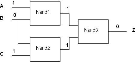
The initial value of the input vector (A, B, C) is (1, 0, 1); the output of each gate is shown (and the initial values have been chosen so that the behavior of the circuit is consistent and stable.)
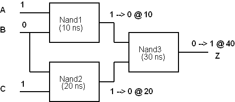
The goal of the simulator is to predict what will happen to various signals if one (or more) inputs change. Suppose, for example, that the input vector becomes (1, 1, 1). Basic boolean logic tells us that the output Z is now 1; i.e.:
Z = AB + BC = 1*1 + 1*1 = 1The simulator should be able to handle arbitrarily complex circuits (including feedback loops). The simulator should also explicitly take into account gate delays and determine the time of any signal change.
For example, in the example above let us first assume that the gate delays for the three Nand gates are 10, 20 and 30 ns and that input B changes from 0 to 1 at time 0. The first visible effect will be the output of Nand1 which will change from 1 to 0 at time 10 ns. The next effect will be the Nand2 output changing from 1 to 0 at time 20 ns. The final effect (after which the circuit will be stable barring additional input changes) will the the Nand3 output changing from 0 to 1 at time 40 ns.
The event-driven simulation model only does something when a signal changes. (Henceforth, we will use the word Node instead of signal.) These changes are scheduled and are called Events. An Event indicates a new value for some Node scheduled to occur at some specific time.
All pending Events are maintained in a priority queue. The simulation procedes by removing one Event at a time from the queue and computing its consequences which may include the generation of additional Events. This procedure continues until there are no more pending Events.
Let's start with the previous circuit where the intial input vector (A, B, C) is(1, 0, 1) and all other Nodes have been initialized to consistent values. How does the event-driven model behave when the input vector becomes (1, 1, 1)?
From the point of view of the simulator, the input vector itself is of no interest; rather, the changes in any of the Nodes is very much of interest. Here, the change in the B Node: it is scheduled to become 1 at time 0. Hence we add an Event (node:B, value:1, time:0) to the queue
The queue now has one Event in it. The simulator now removes this single Event and computes its consequences.
In this case, since the B Node is an input to both Nand1 and Nand 2, the outputs of these gates needs to be re-computed. Both outputs will become 0, but at different times. Consquently, two new Events are added to the priority queue:
Once the Nand1-output event is handled, a new Event is added to the queue which now contains:
Neither of these Events has any further consequences and the simulation terminates once they have been removed from the queue.
The fundamental classes in the package are:
Consider the simple circuit with the indicated stable and consistent initial Node values.
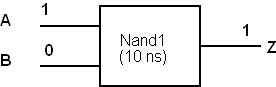
Suppose that both inputs A and B change simultaneously. The inputs to the Nand gate will still have one input at 0 and the other at 1; the output should remain at 1. This will be the case if the Event changing A to 0 is handled before the Event that sets B to 1. However, Events that occur at the same time may be handled in any order. If the B event is handled first, the current algorithm will set the output Z to 0 and, as soon as it handles the A event (which will occur at the same “time”), it will set Z back to its correct value of 1.
In short, there will be a zero-time pulse at the Nand output: we call this a “glitch”.
There are many possible ways that the simulation algorithm could be modified to eliminate these glitches. For example, the Simulator could check if there was a previous Event for the same Node at the same time and delete one or both of them. (This approach would eliminate a glitch after the Events generated had been produced but before the offending glitch Events were processed.)
The recommended solution, however, is:
This version of the simulation engine does not solve the glitch problem in the “correct” way. Rather, we find a work-around (or kludge) solution.
The work-around solution involves no changes to the Simulation engine or any of its classes. Rather, we exploit the basic functionality of the engine with a new concrete Block whose sole purpose is to eliminate glitches.
This new class is called OutDamnSpotOut (with apologies to W. Shakespeare and Lady Macbeth). You can insert this Block (which has zero delay) at the output of any Block that may produce undesireable glitches.
Refer to the OutDamnSpotOut documentation for more information.
My reasons for the work-around:
Having only Boolean Node values (1 and 0) limits the usfulness of the simulator. For example, devices with tri-state or open-drain (collector) outputs cannot be simulated directly. Other Node values such as hi-Z, weak-0 and weak-1 could solve this problem. Additional values such as unknown, rising and falling could also be useful.
Note that there is a work-around for tri-state devices: for a set of tristate outputs connected to the same Node, treat each as an ordinary output and connect each output to a multiplexor input. Use the tri-state control signals to select the multiplexor input and connect the its output to the original Node driven by the tri-state devices.
The current delay model is very simple (and this is done on purpose to achieve simplicity). The model assumes:
We use the term “ballistic delay” to describe a delay element whose input is copied to its output exactly delay-time later. For example, if a 10 ns delay element has an input pulse of 0.00001 ns, that extremely short pulse will be echoed at the output 10 ns later.
Real circuits do not work like that. (Suppose you build a real inverter with real devices such as transistors and real wires/capacitors/inductors/resistors and measure the delay between an input change and an output change. If your oscilloscope indicates a 10 ns delay, you can reasonably deduce that a 0.00001 ns pulse at the input will be swallowed by the various capacitances in the circuit and never appear at the output.)
In the “inertial delay” model, an input pulse whose duration is less than some specified time (usually some percentage of the delay time) is simply ignored. This model is a better approximation of how real devices behave. (Note that it also includes the ballistic model as a special case: i.e. when the minimum pulse duration to ignore is zero.)
There are possible work-arounds for these limitations using specialized concrete Blocks to emulate the inertial delay model or asymmetric delays using the existing built-in ballistic delay model. The techniques used in the OutDamnSpotOut Block could be used to do this.
Not only do real circuit elements usually work using an inertial delay model, they also have additional timing specifications such as setup, hold, rise and fall times.
While all of these could be accomodated (at least in principle) within the current model (by using various specialized Blocks), it may well be better to incorporate some of these parameters directly into the simulation engine.
These issues are particularly important when a Block has an input that is edge sensitive.
Nothing prevents two outputs being connected together.
The current specification for valid Node names is too general.
The bug involving Node naming conventions should be fixed.
The most important limitation is the restriction of Node values to pure Boolean values. Adding additional possibilities to support tri-state outputs has the highest priority. This would also be the time to address the “output cross-connection” bug.
Many of the remaining limitations can be addressed at the user interface level and by creating special blocks based on the current ballistic delay model to emulate other delay models.
It would be very nice if the simulator (either the engine itself or the user-interface or some combination of the two) could throw an Exception when some constraint (such as hold/setup time violation or short-cicuiting active outputs) were violated.
Despite the bugs and limitations of the current simulation engine, the bigger problem at the present time is the poor quality of the user interface(s).
The simulator itself (the digsim package) is meant to provide the necessary mechanisms to implement any user-interface policy. It is important to retain this division between mechanism and policy; in particular, care should be taken when adding features to the simulation engine that could be dealt with at the user-interface level.
The simulator core was designed and implemented in 1997. This initial core was used as a demonstration in a course that year (and never used again). In 1999, I re-wrote the core design in C using various Abstract Data Type conventions appropriate to that non-object-oriented language. The C version has been used in lab projects at the second-year level (a basic course on data stuctures and algorithms) since then.
In February 2004 I was teaching a third-year course on object-oriented design (with Java as the primary language) when I remembered that I had written a prototypical digital circuit simulator using Java in the distant past. After digging through archives, I found the original source code and design documentation
I was not too embarassed by the quality of the design/analysis/implementation and used the old code as a starting point for lab projects. I also cleaned up the old design and started work on a user-interface package.
This is the result.
|
||||||||||
| PREV PACKAGE NEXT PACKAGE | FRAMES NO FRAMES | |||||||||